Note
Go to the end to download the full example code
EDB: fully parametrized design#
This example shows how you can use HFSS 3D Layout to create and solve a parametric design.
Perform required imports#
Perform required imports, which includes importing the Hfss3dlayout object
and initializing it on version 2023 R2.
import pyaedt
import os
Set non-graphical mode#
Set non-graphical mode. The default is False.
non_graphical = False
Launch EDB#
Launch EDB.
aedb_path = os.path.join(pyaedt.generate_unique_folder_name(), pyaedt.generate_unique_name("pcb") + ".aedb")
print(aedb_path)
edb = pyaedt.Edb(edbpath=aedb_path, edbversion="2023.2")
D:\Temp\pyaedt_prj_BSL\pcb_5033PM.aedb
Define parameters#
Define the parameters.
params = {"$ms_width": "0.4mm",
          "$sl_width": "0.2mm",
          "$ms_spacing": "0.2mm",
          "$sl_spacing": "0.1mm",
          "$via_spacing": "0.5mm",
          "$via_diam": "0.3mm",
          "$pad_diam": "0.6mm",
          "$anti_pad_diam": "0.7mm",
          "$pcb_len": "30mm",
          "$pcb_w": "5mm",
          "$x_size": "1.2mm",
          "$y_size": "1mm",
          "$corner_rad": "0.5mm"}

for par_name in params:
    edb.add_project_variable(par_name, params[par_name])
Define stackup layers#
Define the stackup layers from bottom to top.
layers = [{"name": "bottom", "layer_type": "signal", "thickness": "35um", "material": "copper"},
          {"name": "diel_3", "layer_type": "dielectric", "thickness": "275um", "material": "FR4_epoxy"},
          {"name": "sig_2", "layer_type": "signal", "thickness": "35um", "material": "copper"},
          {"name": "diel_2", "layer_type": "dielectric", "thickness": "275um", "material": "FR4_epoxy"},
          {"name": "sig_1", "layer_type": "signal", "thickness": "35um", "material": "copper"},
          {"name": "diel_1", "layer_type": "dielectric", "thickness": "275um", "material": "FR4_epoxy"},
          {"name": "top", "layer_type": "signal", "thickness": "35um", "material": "copper"}]


# Create EDB stackup.
# Bottom layer
prev = None
for layer in layers:
    edb.stackup.add_layer(layer["name"], base_layer=prev, layer_type=layer["layer_type"], thickness=layer["thickness"],
                                          material=layer["material"])
    prev = layer["name"]
Create padstack for signal via#
Create a parametrized padstack for the signal via.
signal_via_padstack = "automated_via"
edb.padstacks.create(
            padstackname=signal_via_padstack,
            holediam="$via_diam",
            paddiam="$pad_diam",
            antipaddiam="",
            antipad_shape="Bullet",
            x_size="$x_size",
            y_size="$y_size",
            corner_radius="$corner_rad",
            start_layer=layers[-1]["name"],
            stop_layer=layers[-3]["name"]
        )
'automated_via'
Assign net names#
# Assign net names. There are only two signal nets.
Place signal vias#
Place signal vias.
edb.padstacks.place(
            position=["$pcb_len/3", "($ms_width+$ms_spacing+$via_spacing)/2"],
            definition_name=signal_via_padstack,
            net_name=net_p,
            via_name="",
            rotation=90.0
)

edb.padstacks.place(
            position=["2*$pcb_len/3", "($ms_width+$ms_spacing+$via_spacing)/2"],
            definition_name=signal_via_padstack,
            net_name=net_p,
            via_name="",
            rotation=90.0,
)

edb.padstacks.place(
            position=["$pcb_len/3", "-($ms_width+$ms_spacing+$via_spacing)/2"],
            definition_name=signal_via_padstack,
            net_name=net_n,
            via_name="",
            rotation=-90.0,
)

edb.padstacks.place(
            position=["2*$pcb_len/3", "-($ms_width+$ms_spacing+$via_spacing)/2"],
            definition_name=signal_via_padstack,
            net_name=net_n,
            via_name="",
            rotation=-90.0,
)


# ###############################################################################
# Draw parametrized traces
# ~~~~~~~~~~~~~~~~~~~~~~~~
# Draw parametrized traces.
# Trace the width and the routing (Microstrip-Stripline-Microstrip).
# Applies to both p and n nets.

width = ["$ms_width", "$sl_width", "$ms_width"]                       # Trace width, n and p
route_layer = [layers[-1]["name"], layers[4]["name"], layers[-1]["name"]]    # Routing layer, n and p

# Define points for three traces in the "p" net

points_p = [
           [["0.0", "($ms_width+$ms_spacing)/2"],
            ["$pcb_len/3-2*$via_spacing", "($ms_width+$ms_spacing)/2"],
            ["$pcb_len/3-$via_spacing", "($ms_width+$ms_spacing+$via_spacing)/2"],
            ["$pcb_len/3", "($ms_width+$ms_spacing+$via_spacing)/2"],
           ],
           [["$pcb_len/3", "($ms_width+$sl_spacing+$via_spacing)/2"],
            ["$pcb_len/3+$via_spacing", "($ms_width+$sl_spacing+$via_spacing)/2"],
            ["$pcb_len/3+2*$via_spacing", "($sl_width+$sl_spacing)/2"],
            ["2*$pcb_len/3-2*$via_spacing", "($sl_width+$sl_spacing)/2"],
            ["2*$pcb_len/3-$via_spacing", "($ms_width+$sl_spacing+$via_spacing)/2"],
            ["2*$pcb_len/3", "($ms_width+$sl_spacing+$via_spacing)/2"],
           ],
           [["2*$pcb_len/3", "($ms_width+$ms_spacing+$via_spacing)/2"],
            ["2*$pcb_len/3+$via_spacing", "($ms_width+$ms_spacing+$via_spacing)/2"],
            ["2*$pcb_len/3+2*$via_spacing", "($ms_width+$ms_spacing)/2"],
            ["$pcb_len", "($ms_width+$ms_spacing)/2"],
           ],
          ]

# Define points for three traces in the "n" net

points_n = [
          [["0.0", "-($ms_width+$ms_spacing)/2"],
           ["$pcb_len/3-2*$via_spacing", "-($ms_width+$ms_spacing)/2"],
           ["$pcb_len/3-$via_spacing", "-($ms_width+$ms_spacing+$via_spacing)/2"],
           ["$pcb_len/3", "-($ms_width+$ms_spacing+$via_spacing)/2"],
          ],
          [["$pcb_len/3", "-($ms_width+$sl_spacing+$via_spacing)/2"],
           ["$pcb_len/3+$via_spacing", "-($ms_width+$sl_spacing+$via_spacing)/2"],
           ["$pcb_len/3+2*$via_spacing", "-($ms_width+$sl_spacing)/2"],
           ["2*$pcb_len/3-2*$via_spacing", "-($ms_width+$sl_spacing)/2"],
           ["2*$pcb_len/3-$via_spacing", "-($ms_width+$sl_spacing+$via_spacing)/2"],
           ["2*$pcb_len/3", "-($ms_width+$sl_spacing+$via_spacing)/2"],
          ],
          [["2*$pcb_len/3", "-($ms_width+$ms_spacing+$via_spacing)/2"],
           ["2*$pcb_len/3 + $via_spacing", "-($ms_width+$ms_spacing+$via_spacing)/2"],
           ["2*$pcb_len/3 + 2*$via_spacing", "-($ms_width+$ms_spacing)/2"],
           ["$pcb_len", "-($ms_width + $ms_spacing)/2"],
          ],
         ]
# ###############################################################################
# Add traces to EDB
# ~~~~~~~~~~~~~~~~~
# Add traces to EDB.

trace_p = []
trace_n = []
for n in range(len(points_p)):
    trace_p.append(edb.modeler.create_trace(points_p[n], route_layer[n], width[n], net_p, "Flat", "Flat"))
    trace_n.append(edb.modeler.create_trace(points_n[n], route_layer[n], width[n], net_n, "Flat", "Flat"))
Create wave ports#
Create wave ports:
edb.hfss.create_differential_wave_port(trace_p[0].id, ["0.0", "($ms_width+$ms_spacing)/2"],
                                            trace_n[0].id, ["0.0", "-($ms_width+$ms_spacing)/2"],
                                            "wave_port_1")
edb.hfss.create_differential_wave_port(trace_p[2].id, ["$pcb_len", "($ms_width+$ms_spacing)/2"],
                                            trace_n[2].id, ["$pcb_len", "-($ms_width + $ms_spacing)/2"],
                                            "wave_port_2")
('wave_port_2', <pyaedt.edb_core.edb_data.ports.BundleWavePort object at 0x000001D9EE029F60>)
Draw ground polygons#
Draw ground polygons.
gnd_poly = [[0.0, "-$pcb_w/2"],
            ["$pcb_len", "-$pcb_w/2"],
            ["$pcb_len", "$pcb_w/2"],
            [0.0, "$pcb_w/2"]]
gnd_shape = edb.modeler.Shape("polygon", points=gnd_poly)

# Void in ground for traces on the signal routing layer

void_poly = [["$pcb_len/3", "-($ms_width+$ms_spacing+$via_spacing+$anti_pad_diam)/2-$via_spacing/2"],
             ["$pcb_len/3 + $via_spacing", "-($ms_width+$ms_spacing+$via_spacing+$anti_pad_diam)/2-$via_spacing/2"],
             ["$pcb_len/3 + 2*$via_spacing",
             "-($ms_width+$ms_spacing+$via_spacing+$anti_pad_diam)/2"],
             ["2*$pcb_len/3 - 2*$via_spacing",
             "-($ms_width+$ms_spacing+$via_spacing+$anti_pad_diam)/2"],
             ["2*$pcb_len/3 - $via_spacing",
             "-($ms_width+$ms_spacing+$via_spacing+$anti_pad_diam)/2-$via_spacing/2"],
             ["2*$pcb_len/3", "-($ms_width+$ms_spacing+$via_spacing+$anti_pad_diam)/2-$via_spacing/2"],
             ["2*$pcb_len/3", "($ms_width+$ms_spacing+$via_spacing+$anti_pad_diam)/2+$via_spacing/2"],
             ["2*$pcb_len/3 - $via_spacing", "($ms_width+$ms_spacing+$via_spacing+$anti_pad_diam)/2+$via_spacing/2"],
             ["2*$pcb_len/3 - 2*$via_spacing", "($ms_width+$ms_spacing+$via_spacing+$anti_pad_diam)/2"],
             ["$pcb_len/3 + 2*$via_spacing", "($ms_width+$ms_spacing+$via_spacing+$anti_pad_diam)/2"],
             ["$pcb_len/3 + $via_spacing", "($ms_width+$ms_spacing+$via_spacing+$anti_pad_diam)/2+$via_spacing/2"],
             ["$pcb_len/3", "($ms_width+$ms_spacing+$via_spacing+$anti_pad_diam)/2+$via_spacing/2"],
             ["$pcb_len/3", "($ms_width+$ms_spacing+$via_spacing+$anti_pad_diam)/2"]]

void_shape = edb.modeler.Shape("polygon", points=void_poly)

# Add ground layers

for layer in layers[:-1:2]:

    # add void if the layer is the signal routing layer.
    void = [void_shape] if layer["name"] == route_layer[1] else []

    edb.modeler.create_polygon(main_shape=gnd_shape,
                                       layer_name=layer["name"],
                                       voids=void,
                                       net_name="gnd")
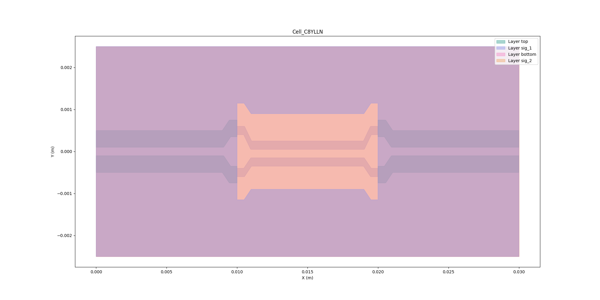
Plot EDB#
Plot EDB.
edb.nets.plot(None)
Save EDB#
Save EDB.
edb.save_edb()
edb.close_edb()
True
Open EDB in AEDT#
Open EDB in AEDT.
h3d = pyaedt.Hfss3dLayout(projectname=aedb_path, specified_version="2023.2",
                          non_graphical=non_graphical, new_desktop_session=True)
Initializing new desktop!
Add HFSS simulation setup#
Add HFSS simulation setup.
setup = h3d.create_setup()
setup.props["AdaptiveSettings"]["SingleFrequencyDataList"]["AdaptiveFrequencyData"]["MaxPasses"] = 3

h3d.create_linear_count_sweep(
    setupname=setup.name,
    unit="GHz",
    freqstart=0,
    freqstop=10,
    num_of_freq_points=1001,
    sweepname="sweep1",
    sweep_type="Interpolating",
    interpolation_tol_percent=1,
    interpolation_max_solutions=255,
    save_fields=False,
    use_q3d_for_dc=False,
)
<pyaedt.modules.SolveSweeps.SweepHFSS3DLayout object at 0x000001D9EDDE2A40>
Set Differential Pairs.#
Define the differential pairs to be used in the postprocessing.
h3d.set_differential_pair(diff_name="In", positive_terminal="wave_port_1:T1", negative_terminal="wave_port_1:T2")
h3d.set_differential_pair(diff_name="Out", positive_terminal="wave_port_2:T1", negative_terminal="wave_port_2:T2")
True
Start HFSS solver#
Start the HFSS solver by uncommenting the h3d.analyze() command.
h3d.analyze()
True
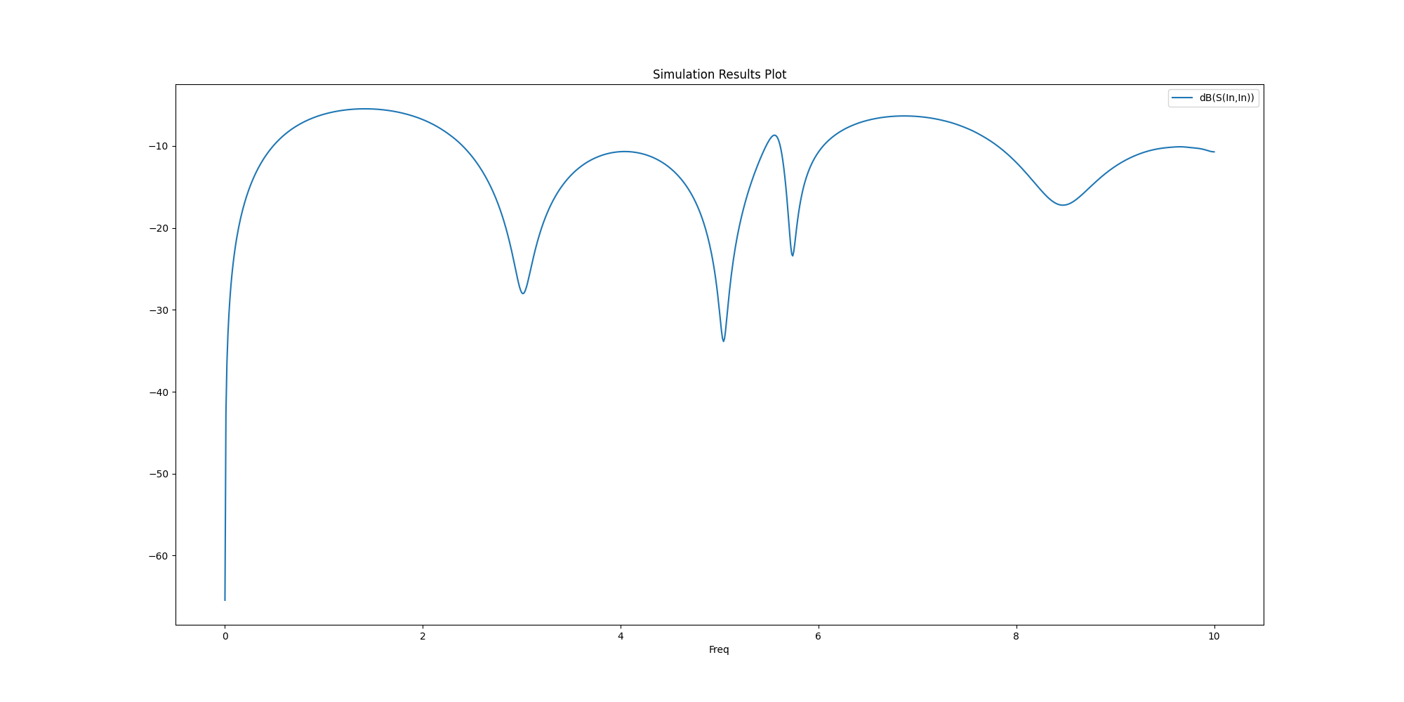
Generate Plot#
Generate the plot of differential pairs.
solutions = h3d.post.get_solution_data(["dB(S(In,In))", "dB(S(In,Out))"], context="Differential Pairs")
solutions.plot()


h3d.release_desktop()
True
Note that the ground nets are only connected to each other due to the wave ports. The problem with poor grounding can be seen in the S-parameters. Try to modify this script to add ground vias and eliminate the resonance.
Total running time of the script: (2 minutes 34.997 seconds)