Note
Go to the end to download the full example code
EDB: geometry creation#
This example shows how you can use EDB to create a layout.
- Final expected project

- Import EDB layout object
Import the EDB layout object and initialize it on version 2023 R2.
D:\Temp\pyaedt_prj_9OL\pcb_AH034U.aedb
Add stackup layers#
Add stackup layers. A stackup can be created layer by layer or imported from a csv file or xml file.
edb.stackup.add_layer("GND")
edb.stackup.add_layer("Diel", "GND", layer_type="dielectric", thickness="0.1mm", material="FR4_epoxy")
edb.stackup.add_layer("TOP", "Diel", thickness="0.05mm")
<pyaedt.edb_core.edb_data.layer_data.StackupLayerEdbClass object at 0x000001D9EDCF2770>
Create signal net and ground planes#
Create a signal net and ground planes.
points = [
    [0.0, 0],
    [100e-3, 0.0],
]
edb.modeler.create_trace(points, "TOP", width=1e-3)
points = [[0.0, 1e-3], [0.0, 10e-3], [100e-3, 10e-3], [100e-3, 1e-3], [0.0, 1e-3]]
edb.modeler.create_polygon(points, "TOP")

points = [[0.0, -1e-3], [0.0, -10e-3], [100e-3, -10e-3], [100e-3, -1e-3], [0.0, -1e-3]]
edb.modeler.create_polygon(points, "TOP")
<pyaedt.edb_core.edb_data.primitives_data.EdbPolygon object at 0x000001D9EDCF6B90>
Create vias with parametric positions#
Create vias with parametric positions.
edb.padstacks.create("MyVia")
edb.padstacks.place([5e-3, 5e-3], "MyVia")
edb.padstacks.place([15e-3, 5e-3], "MyVia")
edb.padstacks.place([35e-3, 5e-3], "MyVia")
edb.padstacks.place([45e-3, 5e-3], "MyVia")
edb.padstacks.place([5e-3, -5e-3], "MyVia")
edb.padstacks.place([15e-3, -5e-3], "MyVia")
edb.padstacks.place([35e-3, -5e-3], "MyVia")
edb.padstacks.place([45e-3, -5e-3], "MyVia")
<pyaedt.edb_core.edb_data.padstacks_data.EDBPadstackInstance object at 0x000001D9ED97F040>
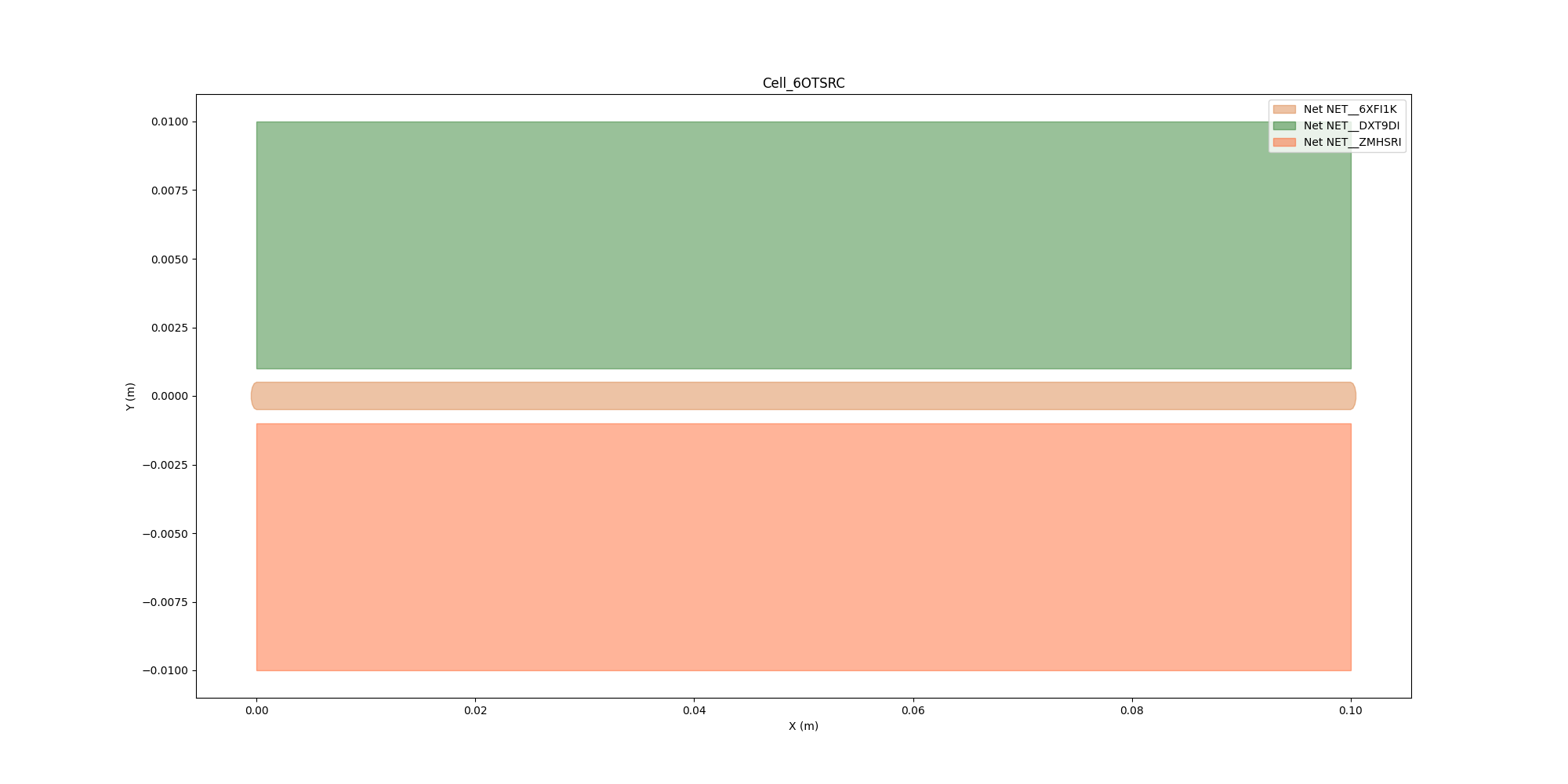
Geometry Plot#
edb.nets.plot(None, color_by_net=True)
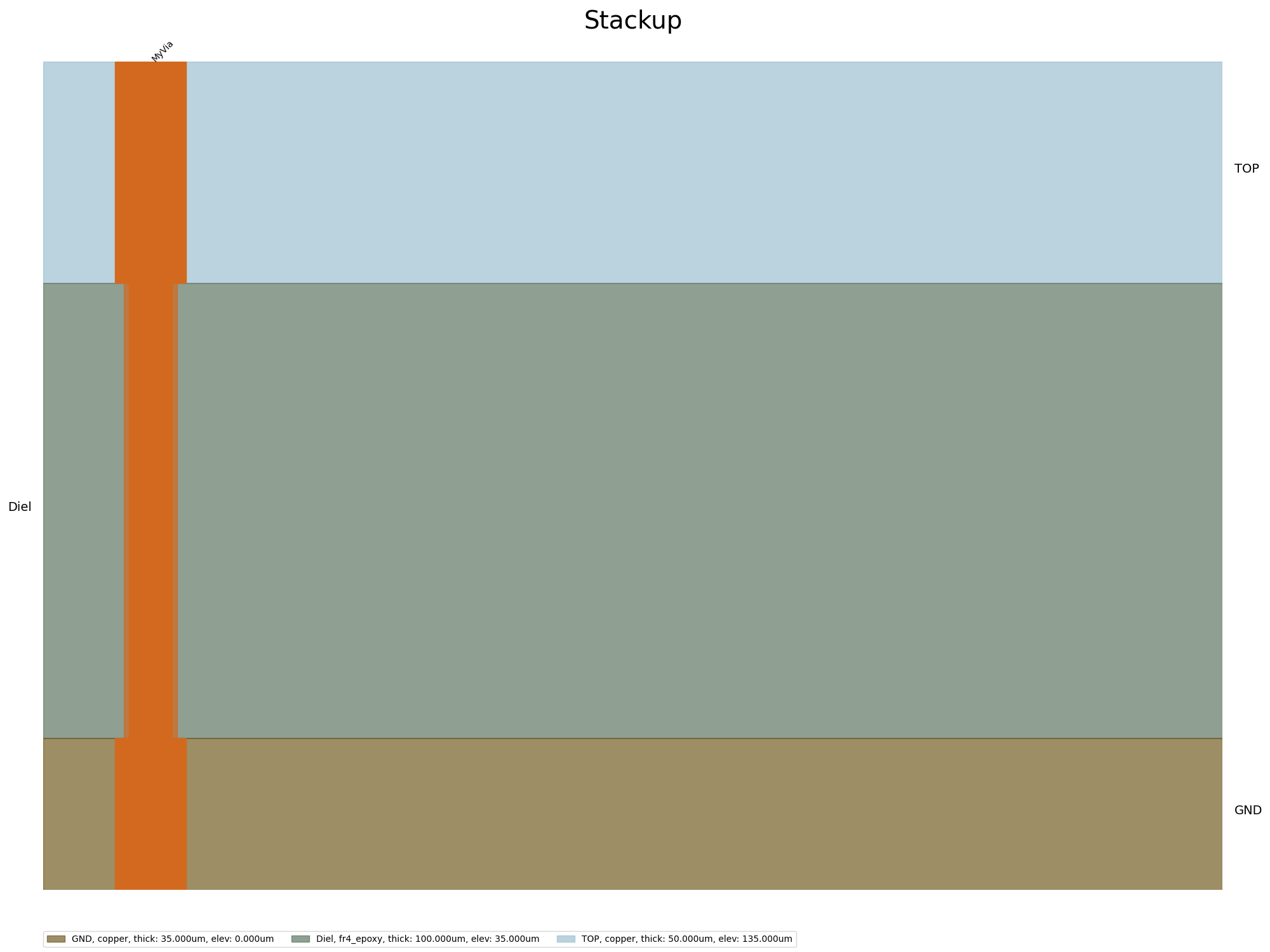
Stackup Plot#
edb.stackup.plot(plot_definitions="MyVia")
<module 'matplotlib.pyplot' from 'C:\\actions-runner\\_work\\pyaedt\\pyaedt\\testenv\\lib\\site-packages\\matplotlib\\pyplot.py'>
Save and close EDB#
Save and close EDB.
EDB saved correctly to D:\Temp\pyaedt_prj_9OL\pcb_AH034U.aedb. You can import in AEDT.
12.749271869659424
Total running time of the script: (0 minutes 12.781 seconds)