Note
Go to the end to download the full example code.
HFSS: 3D Components#
This example shows how you can use PyAEDT to place 3D Components in Hfss and in Hfss 3D Layout.
import os
import pyaedt
Set AEDT version#
Set AEDT version.
aedt_version = "2024.1"
Set non-graphical mode#
Set non-graphical mode.
You can set non_graphical either to True or False.
non_graphical = False
Common Properties#
Set common properties.
trace_width = 0.6
trace_length = 30
diel_height = "121mil"
sig_height = "5mil"
max_steps = 3
freq = "3GHz"
new_session = True
3D Component Definition#
File to be used in the example
component3d = pyaedt.downloads.download_file("component_3d", "SMA_RF_Jack.a3dcomp",)
Hfss Example#
This example will create a stackup in Hfss place a 3d component, build a ground plane, a trace, create excitation and solve it in Hfss.
Launch Hfss#
Launch HFSS application
hfss = pyaedt.Hfss(new_desktop_session=True, specified_version=aedt_version, non_graphical=non_graphical)

hfss.solution_type = "Terminal"
Insert 3d Component#
To insert a 3d component we need to read parameters and then import in Hfss.
comp_param = hfss.get_components3d_vars(component3d)
hfss.modeler.insert_3d_component(component3d, comp_param)
<pyaedt.modeler.cad.components_3d.UserDefinedComponent object at 0x000002263F093970>
Add a new Stackup#
Pyaedt has a Stackup class which allows to parametrize stacked structures.
stackup = hfss.add_stackup_3d()
s1 = stackup.add_signal_layer("L1", thickness=sig_height)
d1 = stackup.add_dielectric_layer("D1", thickness=diel_height)
g1 = stackup.add_ground_layer("G1", thickness=sig_height)
Define stackup extensions#
Define stackup elevation and size. Defines also the stackup origin.
stackup.start_position = "-131mil"
stackup.dielectric_width = "20mm"
stackup.dielectric_length = "40mm"
stackup.dielectric_y_position = "-dielectric_width/2"
stackup.dielectric_x_position = "-dielectric_length/4"
Padstack Definition#
Padstacks are needed to create a clearance around 3d component since intersections are not allowed. There will be 1 padstack for Gnd and 1 for pin.
p1 = stackup.add_padstack("gnd_via", material="cloned_copper")
p1.set_start_layer("L1")
p1.set_stop_layer("G1")
p1.set_all_antipad_value(1.3)
p1.set_all_pad_value(0)
p1.num_sides = 8
p1.add_via(-3.2, -3.2)
p1.add_via(-3.2, 3.2)
p1.add_via(3.2, -3.2)
p1.add_via(3.2, 3.2)
p2 = stackup.add_padstack("signal_via", material="cloned_copper")

p2.set_start_layer("L1")
p2.set_stop_layer("G1")
p2.set_all_antipad_value(0.7)
p2.set_all_pad_value(0)
p2.padstacks_by_layer["L1"].pad_radius = 0.3048
p2.add_via(0, 0)
<pyaedt.modeler.cad.object3d.Object3d object at 0x0000022638C95270>
Trace Definition#
The trace will connect the pin to the port on layer L1.
t1 = s1.add_trace(trace_width, trace_length)
rect1 = hfss.modeler.create_rectangle(orientation=hfss.PLANE.YZ,
                                                 origin=["0.75*dielectric_length", "-5*" + t1.width.name, "0mm"],
                                                 sizes=["15*" + t1.width.name, "-3*" + stackup.thickness.name])
p1 = hfss.wave_port(assignment=rect1, reference="G1", name="P1")
Set Simulation Boundaries#
Define regione and simulation boundaries.
<pyaedt.modules.Boundary.BoundaryObject object at 0x0000022638C96C80>
Create Setup#
Iterations will be reduced to reduce simulation time.
Solve Setup#
Save the project first and then solve the setup.
hfss.save_project()
hfss.analyze()
True
Plot results#
Plot the results when analysis is completed.
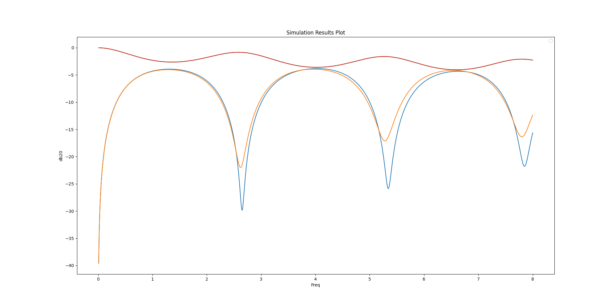
No artists with labels found to put in legend.  Note that artists whose label start with an underscore are ignored when legend() is called with no argument.

<Figure size 2000x1000 with 1 Axes>
Hfss 3D Layout Example#
Previous example will be repeated this time in Hfss 3d Layout. Small differences are expected in layout but results should be similar.
Launch Hfss3dLayout#
Launch HFSS3dLayout application
h3d = pyaedt.Hfss3dLayout()
Add stackup layers#
Add stackup layers.
l1 = h3d.modeler.layers.add_layer("L1", "signal", thickness=sig_height)
h3d.modeler.layers.add_layer("diel", "dielectric", thickness=diel_height, material="FR4_epoxy")
h3d.modeler.layers.add_layer("G1", "signal", thickness=sig_height, isnegative=True)
<pyaedt.modules.LayerStackup.Layer object at 0x000002263F30C8E0>
Place 3d Component#
Place a 3d component by specifying the .a3dcomp file path.
comp = h3d.modeler.place_3d_component(
    component_path=component3d, number_of_terminals=1, placement_layer="G1", component_name="my_connector",
    pos_x=0.000, pos_y=0.000
)
Create signal net and ground planes#
Create a signal net and ground planes.
h3d["len"] = str(trace_length) + "mm"
h3d["w1"] = str(trace_width) + "mm"

line = h3d.modeler.create_line("L1", [[0, 0], ["len", 0]], lw="w1", name="microstrip", net="microstrip")
h3d.create_edge_port(line, h3d.modeler[line.name].top_edge_x, is_wave_port=True, wave_horizontal_extension=15)
<pyaedt.modules.Boundary.BoundaryObject3dLayout object at 0x000002263F421FF0>
Create void on Ground plane for pin#
Create a void.
h3d.modeler.create_circle("G1", 0, 0, 0.5)
<pyaedt.modeler.pcb.object3dlayout.Circle3dLayout object at 0x000002263F1F1060>
Create Setup#
Iterations will be reduced to reduce simulation time.
h3d.set_meshing_settings(mesh_method="PhiPlus", enable_intersections_check=False)
h3d.edit_hfss_extents(diel_extent_horizontal_padding="0.2", air_vertical_positive_padding="0",
                      air_vertical_negative_padding="2", airbox_values_as_dim=False)
setup1 = h3d.create_setup()
sweep1 = h3d.create_linear_count_sweep(setup1.name,
                                       "GHz",
                                       0.01,
                                       8,
                                       1601,
                                       sweep_type="Interpolating")
setup1.props["AdaptiveSettings"]["SingleFrequencyDataList"]["AdaptiveFrequencyData"]["AdaptiveFrequency"] = freq
setup1.props["AdaptiveSettings"]["SingleFrequencyDataList"]["AdaptiveFrequencyData"]["MaxPasses"] = max_steps
Solve Setup#
h3d.analyze()
True
Plot results#
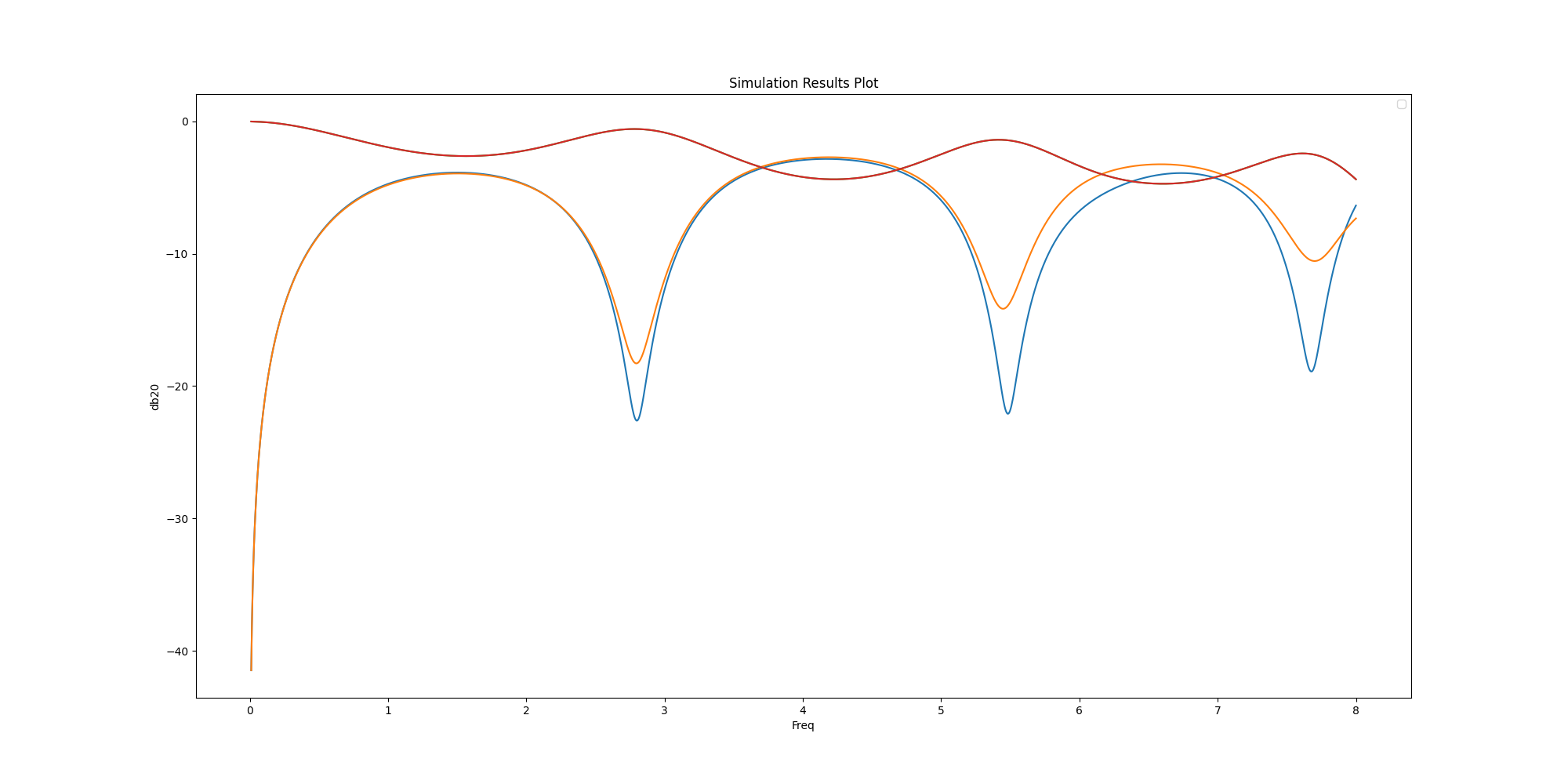
No artists with labels found to put in legend.  Note that artists whose label start with an underscore are ignored when legend() is called with no argument.

True
Total running time of the script: (3 minutes 31.721 seconds)