Note
Go to the end to download the full example code.
HFSS: 3D Components#
This example shows how you can use PyAEDT to place 3D Components in Hfss and in Hfss 3D Layout.
import os
import pyaedt
Set AEDT version#
Set AEDT version.
aedt_version = "2024.1"
Set non-graphical mode#
Set non-graphical mode.
You can set non_graphical either to True or False.
non_graphical = False
Common Properties#
Set common properties.
trace_width = 0.6
trace_length = 30
diel_height = "121mil"
sig_height = "5mil"
max_steps = 3
freq = "3GHz"
new_session = True
3D Component Definition#
File to be used in the example
component3d = pyaedt.downloads.download_file("component_3d", "SMA_RF_Jack.a3dcomp",)
Hfss Example#
This example will create a stackup in Hfss place a 3d component, build a ground plane, a trace, create excitation and solve it in Hfss.
Launch Hfss#
Launch HFSS application
hfss = pyaedt.Hfss(new_desktop=True, version=aedt_version, non_graphical=non_graphical)

hfss.solution_type = "Terminal"
Insert 3d Component#
To insert a 3d component we need to read parameters and then import in Hfss.
comp_param = hfss.get_components3d_vars(component3d)
hfss.modeler.insert_3d_component(component3d, comp_param)
<pyaedt.modeler.cad.components_3d.UserDefinedComponent object at 0x00000187AC949F60>
Add a new Stackup#
Pyaedt has a Stackup class which allows to parametrize stacked structures.
stackup = hfss.add_stackup_3d()
s1 = stackup.add_signal_layer("L1", thickness=sig_height)
d1 = stackup.add_dielectric_layer("D1", thickness=diel_height)
g1 = stackup.add_ground_layer("G1", thickness=sig_height)
Define stackup extensions#
Define stackup elevation and size. Defines also the stackup origin.
stackup.start_position = "-131mil"
stackup.dielectric_width = "20mm"
stackup.dielectric_length = "40mm"
stackup.dielectric_y_position = "-dielectric_width/2"
stackup.dielectric_x_position = "-dielectric_length/4"
Padstack Definition#
Padstacks are needed to create a clearance around 3d component since intersections are not allowed. There will be 1 padstack for Gnd and 1 for pin.
p1 = stackup.add_padstack("gnd_via", material="cloned_copper")
p1.set_start_layer("L1")
p1.set_stop_layer("G1")
p1.set_all_antipad_value(1.3)
p1.set_all_pad_value(0)
p1.num_sides = 8
p1.add_via(-3.2, -3.2)
p1.add_via(-3.2, 3.2)
p1.add_via(3.2, -3.2)
p1.add_via(3.2, 3.2)
p2 = stackup.add_padstack("signal_via", material="cloned_copper")

p2.set_start_layer("L1")
p2.set_stop_layer("G1")
p2.set_all_antipad_value(0.7)
p2.set_all_pad_value(0)
p2.padstacks_by_layer["L1"].pad_radius = 0.3048
p2.add_via(0, 0)
<pyaedt.modeler.cad.object3d.Object3d object at 0x00000187AA887AC0>
Trace Definition#
The trace will connect the pin to the port on layer L1.
t1 = s1.add_trace(trace_width, trace_length)
rect1 = hfss.modeler.create_rectangle(orientation=hfss.PLANE.YZ,
                                                 origin=["0.75*dielectric_length", "-5*" + t1.width.name, "0mm"],
                                                 sizes=["15*" + t1.width.name, "-3*" + stackup.thickness.name])
p1 = hfss.wave_port(assignment=rect1, reference="G1", name="P1")
Set Simulation Boundaries#
Define regione and simulation boundaries.
<pyaedt.modules.Boundary.BoundaryObject object at 0x00000187AA886860>
Create Setup#
Iterations will be reduced to reduce simulation time.
Solve Setup#
Save the project first and then solve the setup.
hfss.save_project()
hfss.analyze()
True
Plot results#
Plot the results when analysis is completed.
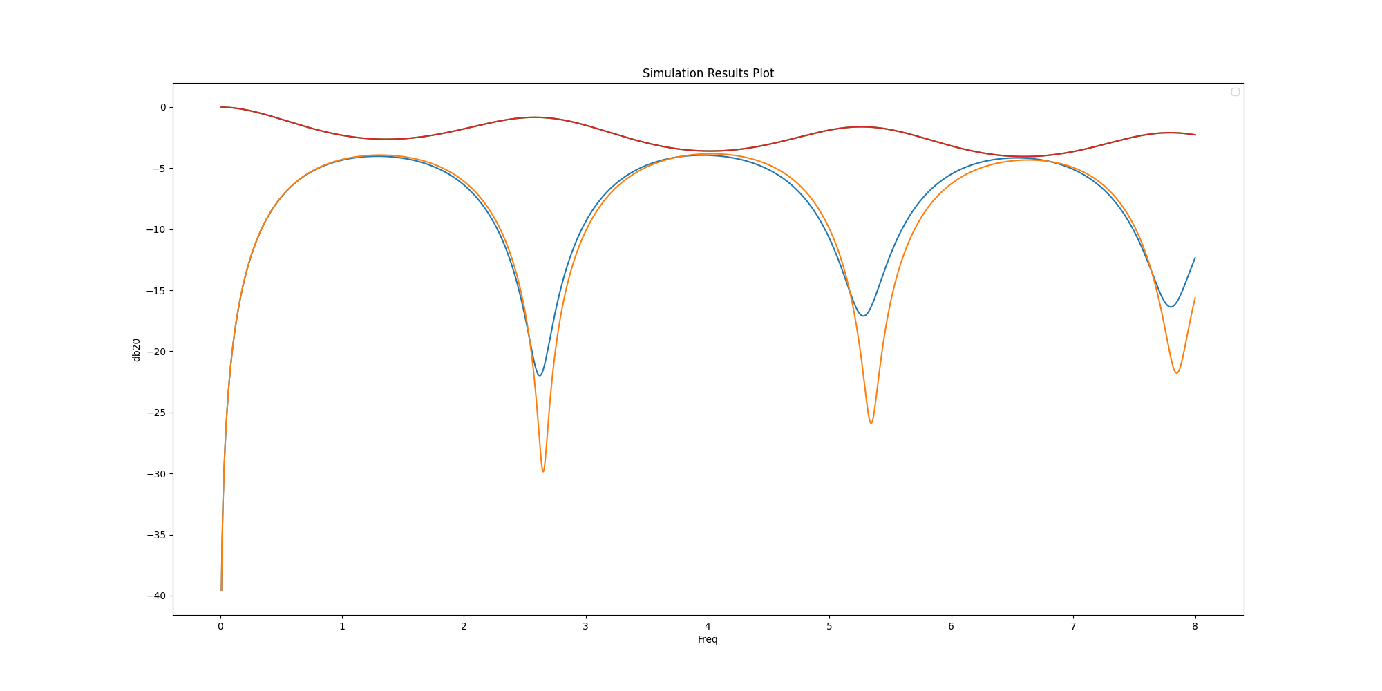
<Figure size 2000x1000 with 1 Axes>
Hfss 3D Layout Example#
Previous example will be repeated this time in Hfss 3d Layout. Small differences are expected in layout but results should be similar.
Launch Hfss3dLayout#
Launch HFSS3dLayout application
h3d = pyaedt.Hfss3dLayout()
Add stackup layers#
Add stackup layers.
l1 = h3d.modeler.layers.add_layer("L1", "signal", thickness=sig_height)
h3d.modeler.layers.add_layer("diel", "dielectric", thickness=diel_height, material="FR4_epoxy")
h3d.modeler.layers.add_layer("G1", "signal", thickness=sig_height, isnegative=True)
<pyaedt.modules.LayerStackup.Layer object at 0x00000187FF5F65C0>
Place 3d Component#
Place a 3d component by specifying the .a3dcomp file path.
comp = h3d.modeler.place_3d_component(
    component_path=component3d, number_of_terminals=1, placement_layer="G1", component_name="my_connector",
    pos_x=0.000, pos_y=0.000
)
Create signal net and ground planes#
Create a signal net and ground planes.
h3d["len"] = str(trace_length) + "mm"
h3d["w1"] = str(trace_width) + "mm"

line = h3d.modeler.create_line("L1", [[0, 0], ["len", 0]], lw="w1", name="microstrip", net="microstrip")
h3d.create_edge_port(line, h3d.modeler[line.name].top_edge_x, is_wave_port=True, wave_horizontal_extension=15)
<pyaedt.modules.Boundary.BoundaryObject3dLayout object at 0x00000187AA92F610>
Create void on Ground plane for pin#
Create a void.
h3d.modeler.create_circle("G1", 0, 0, 0.5)
<pyaedt.modeler.pcb.object3dlayout.Circle3dLayout object at 0x00000187B9E57640>
Create Setup#
Iterations will be reduced to reduce simulation time.
h3d.set_meshing_settings(mesh_method="PhiPlus", enable_intersections_check=False)
h3d.edit_hfss_extents(diel_extent_horizontal_padding="0.2", air_vertical_positive_padding="0",
                      air_vertical_negative_padding="2", airbox_values_as_dim=False)
setup1 = h3d.create_setup()
sweep1 = h3d.create_linear_count_sweep(setup1.name,
                                       "GHz",
                                       0.01,
                                       8,
                                       1601,
                                       sweep_type="Interpolating")
setup1.props["AdaptiveSettings"]["SingleFrequencyDataList"]["AdaptiveFrequencyData"]["AdaptiveFrequency"] = freq
setup1.props["AdaptiveSettings"]["SingleFrequencyDataList"]["AdaptiveFrequencyData"]["MaxPasses"] = max_steps
Solve Setup#
h3d.analyze()
True
Plot results#
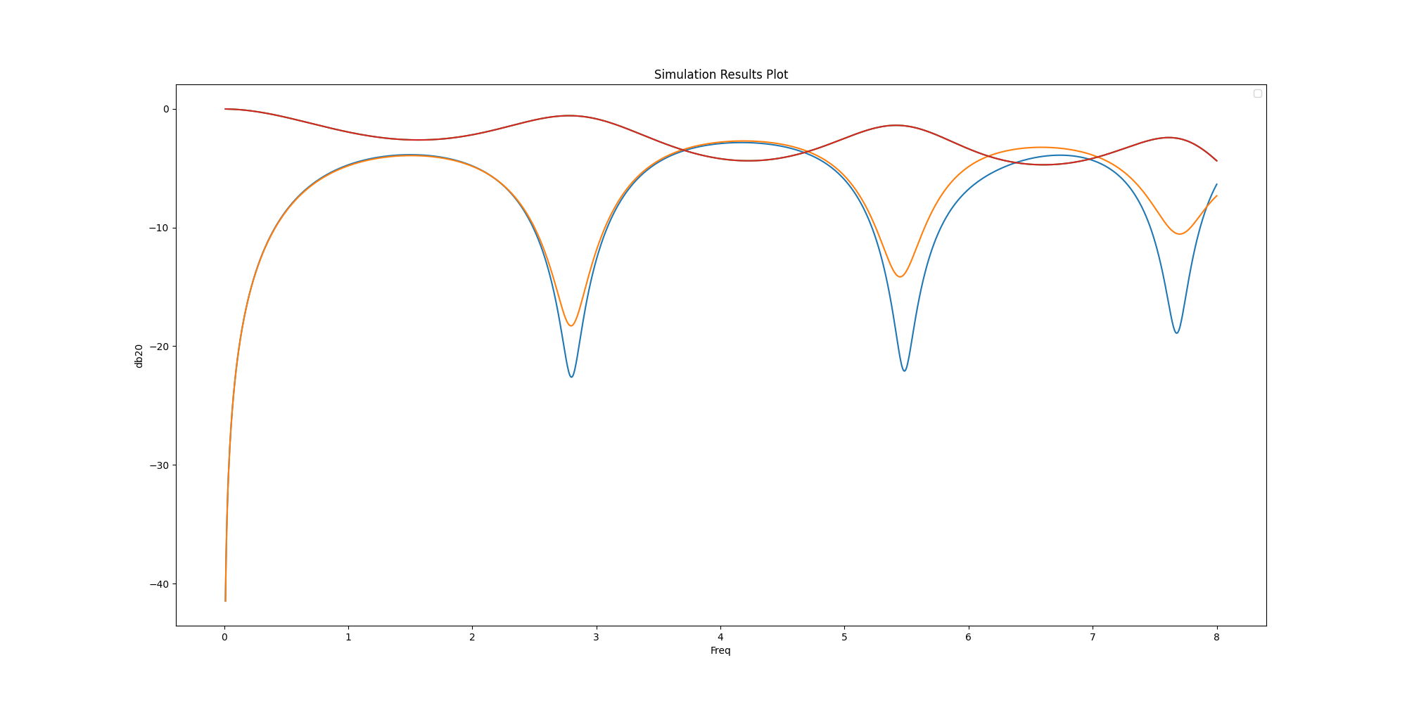
True
Total running time of the script: (3 minutes 14.947 seconds)